Applied Computational Sciences
Computer Aided Engineering Solutions for RF & microwave circuit design
|
Applied Computational Sciences Computer Aided Engineering Solutions for RF & microwave circuit design
|
|
The LINC2 Visual System Architect Enhances RF Architectural Planning, Design and Analysis
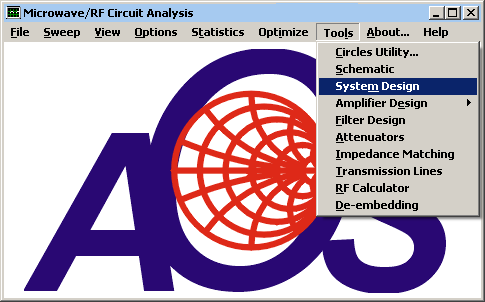
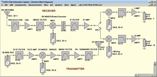
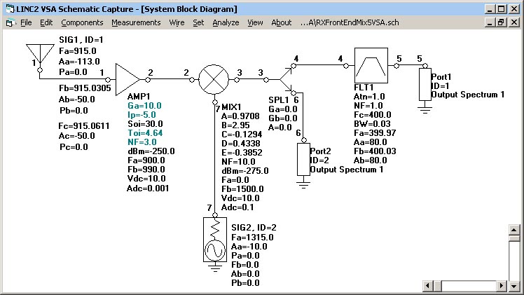
ACS developed the Visual System Architect (VSA) program to automate design and analysis at the system level. LINC2 and the Visual System Architect fulfill the need for software that encompasses the overall product design flow, from high level product specifications to detailed circuit design. Now, with the Visual System Architect addressing product design at the system level and LINC2 Pro automating design at the circuit level, RF and microwave product development can be assured of success by being appropriately driven by system design that connects product specifications to circuit level specifications. Figure 1 shows the LINC2 Tools menu from which both LINC2 Pro and LINC2 VSA are launched. The LINC2 VSA offers a large variety of new design and analysis capability for designing at the system level. The program renders obsolete many of the traditional spreadsheet and system cascade calculators once used to analyze system performance. Instead of having to create and maintain a spreadsheet of calculations, the VSA employs the flexibility and ease of use of schematic based system simulation as shown in Figure 2.
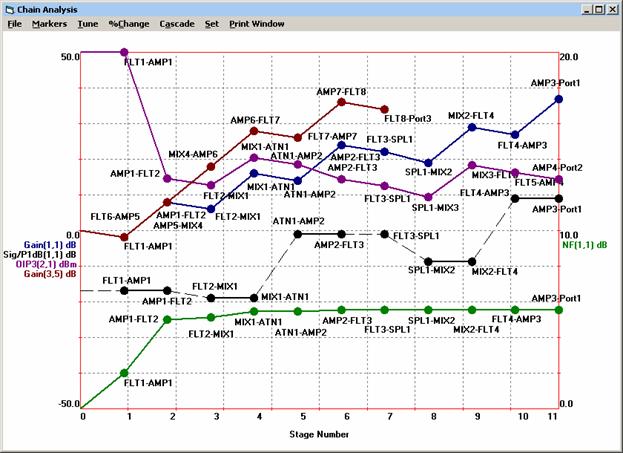
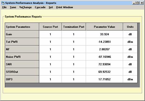
Schematics or system level block diagrams are quickly and easily created from a comprehensive menu of system component behavioral models such as amplifiers, filters, mixers, splitters and attenuators etc. Verifying performance is as simple as clicking the Analyze button. The system schematic allows the user to construct systems of arbitrary topology. Thus, the program is not limited to a single chain of cascaded components. The system simulator can analyze schematics with multiple cascades driven by an equal number of signal power sources. For example, the Visual System Architect can analyze a transmitter and receiver chain simultaneously, each with different signal sources and separate local oscillators for the up-converter and down-converter stages respectively. Plots of power budget, efficiency, gain, IP3 (intercept point), dynamic range, noise power, NF (noise figure) and signal-to-noise ratio (SNR) are just a sampling of the many system performance indicators that are provided on a cumulative stage-by-stage basis. All simulation outputs can be saved to a file or displayed numerically in a table summarizing total system performance (Figure 4). Figure 3 shows a typical cascade budget plot for a transceiver system. Each data point represents a system performance parameter at a circuit node or interface point between stages.
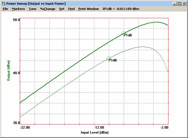
Furthermore, the Visual System Architect goes beyond the traditional budget plots to offer a much wider array of performance measurement methods and analysis tools. For example, Figure 5 shows a power sweep that graphically displays the linear range as well as the P1dB point and compression curve characteristics for the entire system cascade. The Tune menu allows the user to vary any component parameter to immediately see its effect on system linearity including changes to the compression point. The bold curve in Figure 5 represents the initial power sweep while the light curve shows the changes after tuning. The Power Sweep Set > Options menu allows the user to select the range over which input power will sweep. The ability to display an input-output power sweep curve extends to any point in the system, not just to the output port. Thus, the user can probe any internal system node to view the linear range and compression curve characteristics of the system up to and including the selected component.
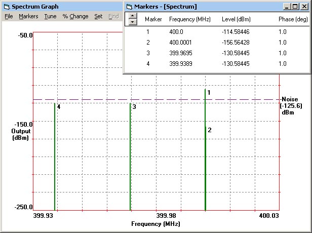
VSA Spectral Domain Analysis One of the most challenging tasks an RF designer is faced with is to ensure that spurious signals are not generated and propagated through the system to places where they may degrade circuit or system performance. Undesired spurious signal products (or spurs) can degrade the sensitivity of a receiver or put a stage into compression and prevent the modulation on a desired signal from passing through the system properly. Spurious signals can mix with other spurs or they can mix with desired signals to create even more undesired spurs that are harmful to system performance, often to the extent of causing the product to fail to meet a number of key specifications. To address the serious issue of spurs, ACS developed the Visual System Architect software with two very powerful analysis tools. One, the Spectrum Analysis display, for viewing the spectral content at any node in the system and the other, the Signal and Spur Viewer Tree, to track the creation and propagation of all spurs throughout the system. The VSA’s spectral domain analysis can plot all the signals and spurs in the system in the form of spectrum analyzer type graphs. To help isolate the cause and path of any unknown spurs, the VSA Spectrum Analyzer Graph can turn any signal source on or off to see which signals or spurs are related to a given source. Like a spectrum analyzer, only better! At first glance the Visual System Architect’s Spectrum Analyzer graph window looks a lot like the screen of a typical spectrum analyzer bench instrument. The spectrum plot displays the entire power spectrum content at any point in the circuit. However, unlike any physical spectrum analyzer instrument, the user can select any component parameter from the Tune menu and adjust its value to see its effect on the production of spectral content. For example, the user could interactively adjust the third order intercept point on a power amplifier to see the effect on the level of 3rd order inter-modulation products at the output. All the signal sources driving the system are listed in the Set menu as well. This allows the user to adjust the input power to the system from any signal source while viewing the resulting change in the levels of all affected signals and spurs.
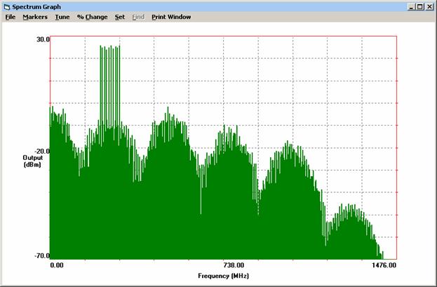
Figure 6 shows the LINC2 VSA’s Spectrum Analyzer view for an amplifier with multi-tone inputs. The number of input signals is limited by the (RAM) memory available for the computer used. However, there are no restrictions on the relative amplitudes of the tones or their spacing. (Note the different amplitudes and spacing for the ten fundamental signals in Figure 6). Thus, one or multiple signals can be input to the system with complete freedom to independently specify the amplitude, frequency and phase of each input signal. The signals input to the system can be represented on the system schematic by signal generators producing up to 3 simultaneous tones per generator. Additionally, a signal generator can be file based so that an entire spectrum of signals can be loaded into the system at once.
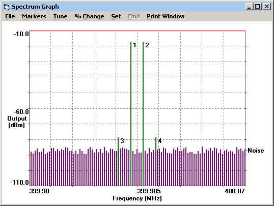
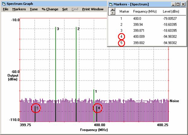
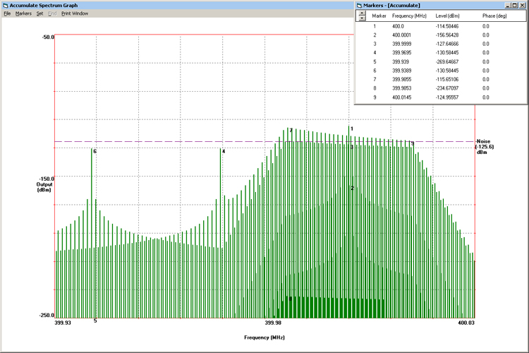
New Spectral Noise Simulations! The VSA’ powerful noise simulation capability lets you see signals and spurs rise above a simulation of the noise floor in a spectrum display that rivals the displays found in actual spectrum analyzer instruments (Figure 7). The VSA also reveals signals or spurs below the noise floor (Figure 8)! Now you can catch impending spurs before they rise above the noise floor - a feature that not even a real spectrum analyzer can do!
LINC2 VSA noise simulation provides the ability to…
In addition to plots of noise figure (NF), the following noise related simulated output measurements are available: Noise Bandwidth Calculations - The noise bandwidth is automatically calculated at every stage in the system - The noise bandwidth (NBW) is adjusted according to the filters used - If filters are not present in the schematic then a detector (or global) NBW can be specified Noise Power Measurement - Total noise power can be plotted (or numerically displayed) for every stage/node SNR (Signal-to-Noise Ratio) Measurement - The Signal-to-Noise Ratio can be plotted (or numerically displayed) for each node SFDR (Spur-free Dynamic Range) Measurement - The SFDR can be plotted (or numerically displayed) for each system stage/node
The VSA Signal Tree- Unique System Signal and Spur Viewer The Visual System Architect provides unique user access to a detailed analysis of every signal and spur in the entire system. The System Signal and Spur Viewer window automatically organizes all these signals and spurs into a tree structure that provides nearly instant access to detailed information on any signal anywhere in the system (as shown in Figure 9). At the highest level in the signal tree is a list of all the signals present at a given node (the output node, for example). Click on any one of these signals and the next level in the tree opens for that signal. A list of all the signals involved in the creation of the selected signal are displayed at this next lower level in the tree. Clicking the “+” symbol in front these “ancestor” signals displays the next level of signals - all the signals involved in creating the selected ancestor. This process continues down to the end (or lowest level) of the branch where the origin of the signal is located. The process of navigating the VSA Signal Tree is similar to the familiar file and folder navigation tree found in the Windows Explorer/File Browser. Each Signal Uniquely Identified Preceding every signal in the list is a numerical tag that uniquely identifies the signal. The signal identifier tag is comprised of three numbers of the form (Source, Node, Index) that uniquely identifies each signal according to the Source that was the ultimate origin of the signal, the Node at which the signal exists and the Index that identifies this signal among the array of signals that are present at this node. Moreover, any signal at any node along the path can be right clicked to reveal its amplitude, frequency and phase (as displayed directly below the signal tree). Expansion of the signal tree (clicking through a branch in the tree) yields the path a particular component of the signal travels from its source to arrive at the point of observation.
All New Phase Noise Simulations! New LINC2 Visual System Architect
features and capabilities add phase noise analysis by accepting into the
simulation signal files that contain the signal along with samples of its double
sideband phase noise. The simulation can be directed to apply the
signal/phase noise file to any signal source in the schematic (for example the
LO in Figure 10 below), sweep through the file's signal/phase noise profile
while accumulating the simulation results into a spectrum display.
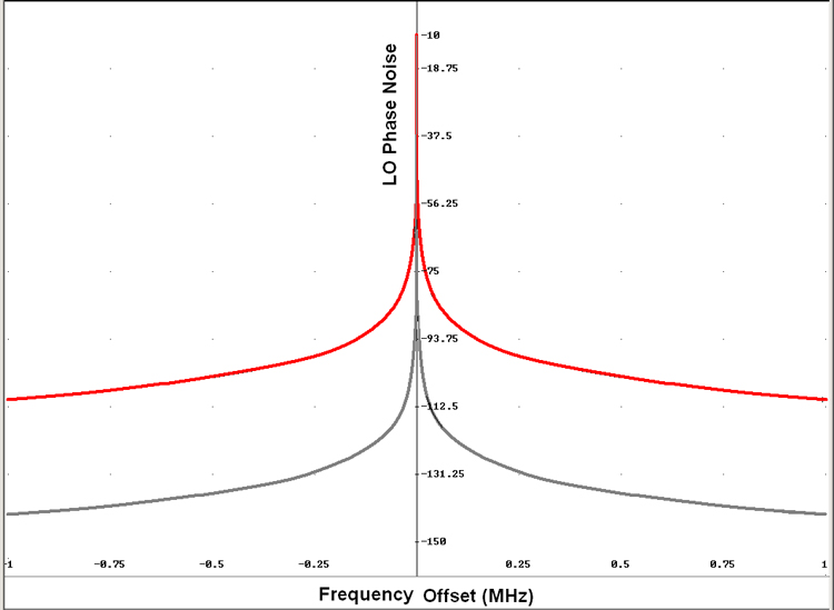
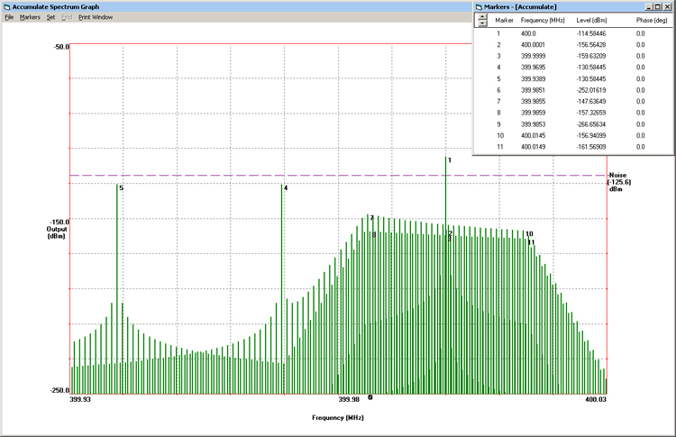
Applying the phase noise from the lower (grey) plot from Figure 12 to the LO yields the simulation results of Figure 14. The simulation results of Figure 14 show more than 30 dB improvement in in-band phase noise relative to what was found in Figure 13. Comparing Figure 14 to Figure 13 demonstrates that for a given offset, the in-band phase noise (due to reciprocal mixing) improves dB for dB with the improvement in LO phase noise. Whereas in Figure 13 (simulation with poor phase noise LO) the in-band phase noise exceeded the thermal noise floor to become the limiting factor in SNR, in Figure 14 the in-band phase noise is more than 20 dB below the noise floor and therefore does not contribute to the SNR.
The LINC2/VSA Software Suite The Visual System Architect from ACS includes the stage-by-stage cumulative system budget analyses that are essential to successful system design, analysis, system performance verification and report generation. Full spectral domain analysis provides a spectrum analyzer view of all signals and spurs at any point in the system. With the System Signal and Spur Viewer the user can trace any signal or spur through the system back to its source. System design and analysis productivity is enhanced by the flexibility and ease of use of schematic based system simulation. The ability to drag and drop circuit or system components onto the schematic page from an inclusive menu of component models allows the user to quickly construct system diagrams of arbitrary topology. “What if” scenarios can quickly and easily be tested by simply dragging components into new configuration lineups. Documenting system performance and report generation is easy since the VSA software can export the tabular data from the Reports page as well as all data from Cascade Budget Analysis, Power Sweeps, and Spectrum Analysis Graphs to standard CSV files that can be immediately imported into spreadsheets such as Excel. The data is also compatible with a wide variety of other programs through the common CSV format. The VSA maintains a common user interface between system level and circuit level schematics making it easy to transition from system design to detailed circuit design and back without having to learn or become reacquainted with a different operational behavior. LINC2 system simulation and circuit simulation is also operationally similar and both have the same easy to use operator interface- simply enter schematic, set output options, click Analyze and View Results/Reports. LINC2 offers exact circuit synthesis, schematic capture, circuit simulation, circuit optimization and yield analysis in a single affordable design environment. Now, with the Visual System Architect, RF and microwave circuit design can be suitably driven by system design that connects product specifications to circuit level specifications. The Visual System Architect software provides interactive (real time) tuning at the system level to help ensure that a product will comply with required specifications before valuable resources are committed to detailed circuit design and prototyping. |
Send mail to
linc2 @ appliedmicrowave.com with questions or comments
about this web site.
|