|


|
|
|

|
|
DECEMBER
2001
RF Design
Software Combines Synthesis and Simulation
by Dale Henkes, Applied Computational Sciences
|
|
|
Perhaps the most efficient way to
create a new circuit design would be to let a circuit synthesis program
create the initial design from a set of specifications. The circuit thus
created would serve as the initial or “approximate” solution which could
then be entered into a circuit simulator for verification. During the
simulation and verification process it might be necessary to modify the
circuit to include parasitic elements and/or the conversion of ideal
components to physical or practical ones.
There are a number of popular RF CAE/CAD software packages on the market
today. Most provide circuit simulation in the frequency or time domain or
both. Some provide modules that are capable of synthesizing a specific
circuit or sub-circuit. These are usually provided as upgrades or add-on
modules for an additional cost. The LINC2 RF CAE program from Applied
Computational Sciences offers an integrated design environment for the
design (synthesis) and simulation of RF and microwave circuits. With
LINC2 a project can flow smoothly from design to verification because the
program couples schematic capture and a suite of RF design tools to a
powerful simulator engine. LINC2 is a high performance, low cost, RF
design solution which includes schematic capture and all synthesis tools
for under $500.00.
When the software provides simulation only, the design becomes a process
of trial and error. Some simulation packages provide circuit templates or
example schematics of common circuits. However, there is no guarantee
that the circuit topology provided will satisfy a new set of
specifications, even after employing optimization. Consider, for example,
the output matching network for an RF amplifier. One of the most
economical circuits for narrow-band matching is the two-element “L”
network. There is a form of “L” network that will match any complex
source to any other complex load. However, if one of these “L”
configurations is borrowed from an existing design or template and
applied to a new device and/or load it is likely to fail to provide an
impedance match, even after lengthy attempts to use an optimizer. The
designer may not realize the futility of the attempt until a great deal
of time has been expended.
Starting a design with synthesis is not only a more direct approach, but
the well-designed synthesis program will only provide circuit topologies
that will meet the specifications. Some times the component values
generated may not be practical, but at least they are returned almost
immediately for review. Often, several alternative circuit topologies are
returned by the synthesis program so that the user can choose the one
with the most realizable component values.
|
|
|
|
|
|
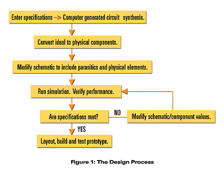
The synthesis module may be linked to a simulator so
that the newly created circuit can be analyzed against a much broader set
of performance criteria using a larger set of analysis tools. For
example, the circuit simulator can check if a design is manufacturable by
looking at its sensitivity to component tolerances using Monte Carlo
analysis. Also, parasitic elements can be modeled and added to the
schematic and ideal components can be replaced by physical ones. The
simulator can then be run and these effects can be reduced or eliminated
by tuning or optimization. The process flow, starting with synthesis, is
shown in Figure 1.
LNA Design Example
This following example illustrates the design process outlined in Figure
1. Proposed is the design of an LNA (low noise amplifier) operating at
2400 MHz with the following specifications:
1. Use the NEC NE76038 GaAs MESFET biased at Vds = 3V and Id = 10 mA.
2. Operate with a source impedance of 75 ohms and a load impedance of 50
ohms.
3. The amplifier must be uncondi- tionally stable at the operating
frequency.
4. Design for a gain greater than 13 dB at 2400 MHz.
5. The noise figure (NF) should be less than 1 dB.
6. Use distributed (microstrip) matching networks.
7. Provide a conjugate output match (|S22| > 20 dB).
The LINC2 Circles Utility is an amplifier design module that
automatically synthesizes input and output networks for a transistor or
FET based on interactive displays of gain, noise figure, and stability
circles overlaid on the Smith Chart. The circles and other related
printed data provide the user with a great deal of pre-synthesis
information designed to guide the user to the best choice of matching
networks for a particular design goal. The program then provides the user
with a menu list of matching circuit topologies (including L, PI, T and
various transmission line/stub forms). The use of this tool to achieve
the above specifications will be demonstrated next.
|
|
|
|
|
|
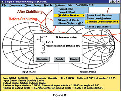
Figure 2
click
image to enlarge
|
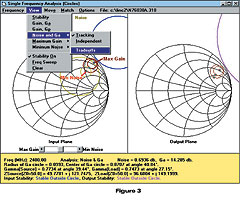
Figure 3
click
image to enlarge
|
|
|
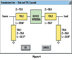
Figure 4
click
image to enlarge
|
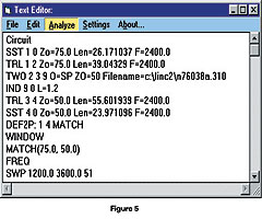
Figure 5
click
image to enlarge
|
|
|
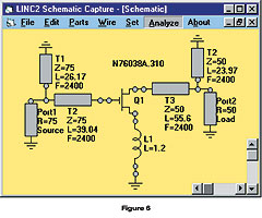
Figure 6
click
image to enlarge
|
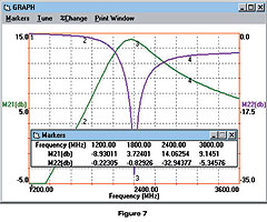
Figure 7
click
image to enlarge
|
|
|
Select the FET type
and operating conditions (specification 1):
The first step is to load the S-parameter file for the NE76038 FET. When
the S-parameter file is read from the disk the noise parameters are
automatically extracted from the file and used to calculate the noise
data. The operating frequency is then set to 2400 MHz via the “Frequency”
menu.
Design for a given source and load impedance (specification 2):
Setting the source (generator) impedance to 75 ohms is accomplished by
selecting “Target Z0in” from the “Options” menu and entering the new
value (Figure 2). The default is 50 ohms, so it is not necessary to
change the “Target Z0out”.
Design the amplifier for unconditional stability (specification 3):
Selecting “Stability” from the “View” menu generates input and output
stability circles on Smith Charts in their respective planes. Initially
the stability circles cut into the Smith Chart and the program reports
that the stability factor, K, is less than 1, a condition for potential
instability. It is not always necessary to correct this condition if the
terminating impedances can be maintained at a safe distance from the
unstable regions defined by the circles. However, rendering the device
unconditionally stable has other advantages that include making it
possible to match both input and output ports simultaneously or at least
achieving a more desirable match if matching both ports is not intended.
LINC2 provides several ways to automatically stabilize a device. As shown
in the “Options > Stabilize Device” menu in Figure 2, the device can
be loaded with a series or shunt resistor or an inductance can be applied
to the common (FET source) lead. For this example, inserting a small
amount of inductance between the source lead and ground was chosen. The
program automatically determined that about 1 nH was the minimum amount
of inductance required. Applying 1.2 nH produced some additional margin
(K>1 and (³<1) as shown in the data box at the bottom of the
window. Also, the stability circles no longer cut into the Smith Chart.
They have been pushed out past the outer edge of the chart as shown in
Figure 2. In addition to meeting the goal of unconditional stability at
the operating frequency, it will be necessary to ensure out-of-band
stability as well. This can be accomplished by designing bias and DC
supply feeds that have little effect in-band but provide stable
terminations out-of-band.
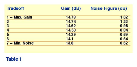
Design for a gain greater than 13 dB (specification 4):
Selection of a target for gain cannot be made independent of noise
considerations. Typically, a tradeoff exists between producing more gain
and the noise figure that can be achieved at that value of gain. The
LINC2 program facilitates making gain-noise tradeoffs by providing a
slider control that allows continuous adjustments (tradeoffs) between
maximum gain and minimum noise figure. Selecting “Noise and Ga >
Tradeoffs” from the “View” menu produces simultaneous displays of gain
and noise data as shown in Figure 3. Moving the gain-noise control from
max gain to min noise produces the data in Table 1.
Design for a noise figure (NF) less than 1 dB (specification 5):
As mentioned above, noise figure can usually be traded for gain and vice
versa. Table 1 indicates that about 1 dB of gain can be traded for 1 dB
of noise figure. Sliding the gain-noise control to its midpoint position
generated the data on line 5 of Table 1. The corresponding input match is
plotted as a point located between the points labeled Max Gain and Min
Noise on the input Smith Chart (Figure 3). This was the position taken in
this example to complete the design and achieve the required
specifications.
Use distributed (microstrip) matching networks (specifications 6 and
7):
At this point the program has all of the information it needs to complete
the design. A menu of matching topologies are available that includes
distributed (transmission line) networks. Selecting “Transmission Line
> Stub and TRL Cascade” from the “Match” menu produces the schematic
shown in Figure 4 with matching networks applied to the device. When the
user selects a particular topology the program automatically calculates
all component values necessary to realize the match points plotted on the
input and output planes (Figure 3). The program links the input and
output planes through a mapping process that generates a conjugate output
match for any input match selected by the user.
Clicking “OK” confirms the selection of this matching topology and
automatically generates the circuit netlist shown in Figure 5. The
corresponding LINC2 schematic shown in Figure 6 represents the initial
synthesized circuit using “ideal” components.
|
|
|
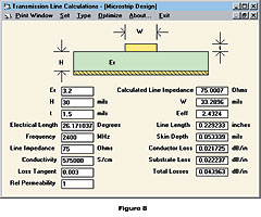
Figure 8
click
image to enlarge
|
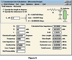
Figure 9
click
image to enlarge
|
|
|
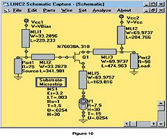
Figure 10
click
image to enlarge
|
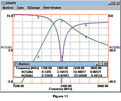
Figure 11
click
image to enlarge
|
|
|
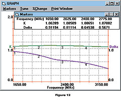
Figure 12
click
image to enlarge
|
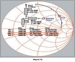
Figure 13
click
image to enlarge
|
|
|
The next step is to replace the
ideal synthesized components with physical ones. But first, we can run a
simulation on the schematic to generate a performance baseline from which
to compare the final circuit with the synthesized one. Figure 7 indicates
that the gain is about 14 dB at 2400 MHz, agreeing closely with the value
predicted by the Circles Utility (from Table 1 and Figure 3, Ga = 14.285
dB). At this point any slight differences are due entirely to the number
of significant digits used for the component values in the simulation.
The output return loss (M22) reported in Figure 7 is nearly ideal at
32.94 dB. We will now see how this performance holds up as the ideal
components are replaced by physical ones.
Synthesize Physical Components
The next step of the process, outlined in Figure 1, is to convert the
ideal components to physically realizable components (microstrip
transmission lines printed on a circuit board substrate). The LINC2
transmission line tool does this automatically as shown in Figure 8 and
9. Figure 8 shows how the physical dimensions of the 75ž shorted stub
(input matching element T1 in Figure 6) are generated. Figure 9 shows how
the 1.2 nH source inductor, L1, is converted to physical printed trace
dimensions for the circuit board material indicated.
After converting the rest of the transmission line elements from
electrical parameters (based on line impedance Z0, degrees of electrical
length, and frequency) to simple physical descriptions of length, L, and
width, W, the schematic is updated as shown in Figure 10. Since the
performance of the amplifier is very sensitive to the way it is grounded,
a ground via (V1 in Figure 10) has also been added to the end of the
source trace to model the effects of a non-ideal ground. Figure 11 shows
the results of rerunning the simulation from the schematic representation
of the “physical” circuit (Figure 10).
Figure 11 indicates that losses in the physical components have reduced
the gain by just over 0.5 dB while the output match has degraded by
almost 10 dB. However, the output match is still very respectable at 23
dB and the gain remains above our 13 dB goal. Stability factors K and ³ in
Figure 12 report that the LNA is unconditionally stable over at least a
1.5 GHz band around the operating frequency.
Since the input match determines the amplifier’s noise figure, a
simulation of just the input network was run to determine if the required
source impedance of 49.8 + J121.8 (from Figure 3) has been preserved in
the final circuit. Marker 3, at 2400 MHz in Figure 13, indicates that the
source impedance remains at 50 + J121 ohms, thus preserving the original
0.7 dB noise figure.
|
|
|
click
image to enlarge
|
|
|
Performance
Summary
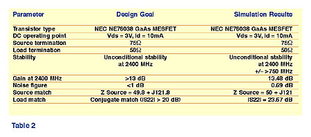
Table 2 lists the design goals (synthesis objectives) and the stimulation
results of the final circuit. All objectives have been met after
replacing the ideal components with the microstrip lines based on the
physical descriptions and taking into account the board and strip losses.
Summary and Conclusions
This article demonstrates how synthesis and simulation can be used
together to speed up the design process. LINC2 enhances the efficiency of
this process by providing a set of synthesis and analysis tools
(including simulation) from within a common design environment. The
design flows smoothly from synthesis to verification because all the data
input, calculations, and displayed output are performed within a single
integrated program. The entire LNA design project presented here, for
example, was performed in only a matter of minutes by the LINC2 computer
program.
LINC2 is a high performance, low cost, RF and microwave design solution
from Applied Computational Sciences, Escondidi, CA. More information on
LINC2 can be found on the Web at www.appliedmicrowave.com
|
|
|